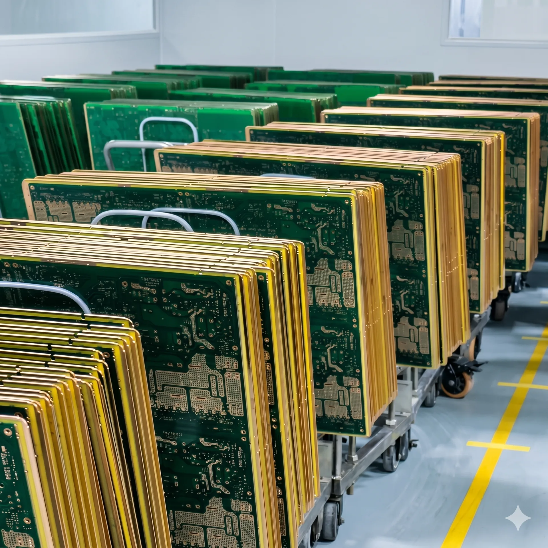
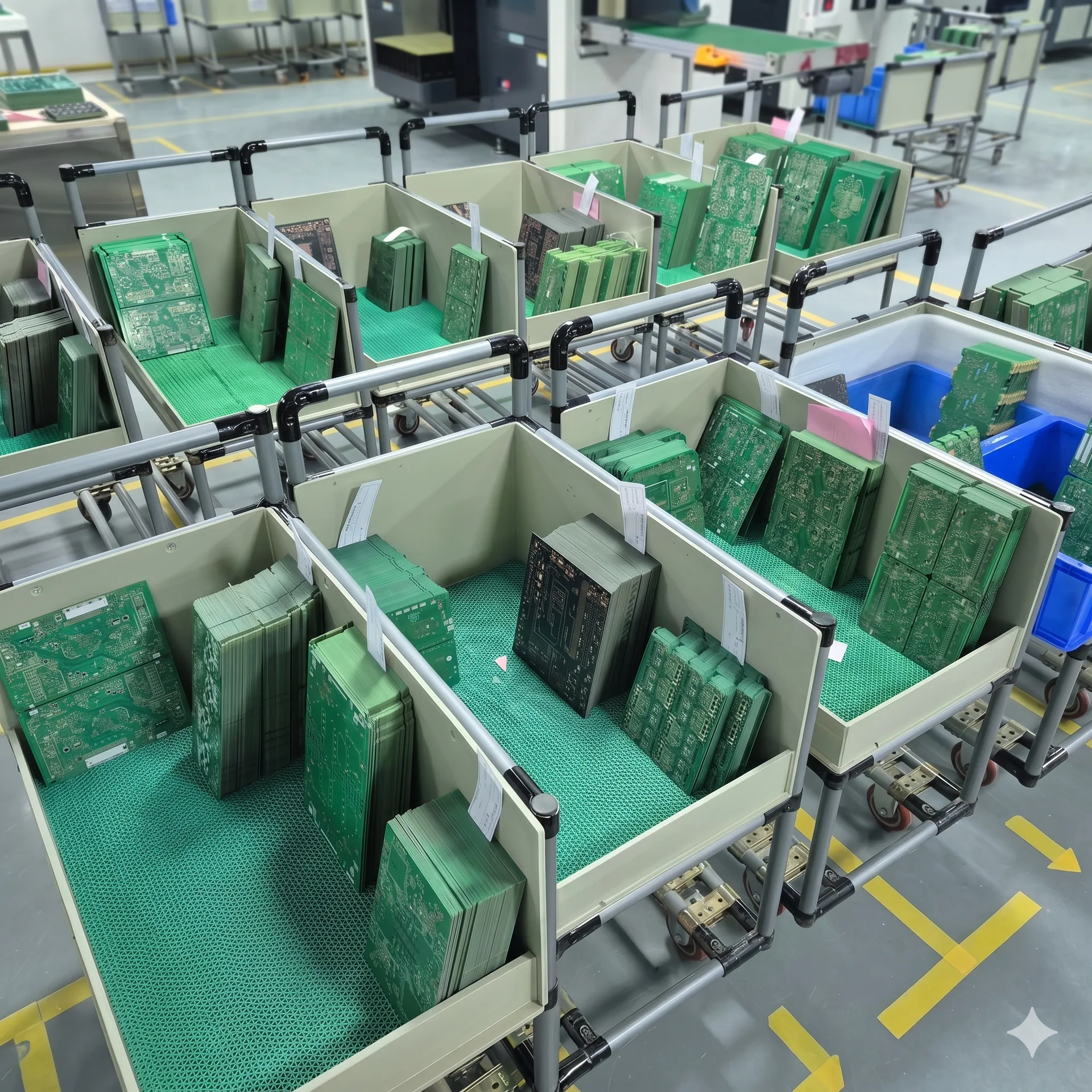
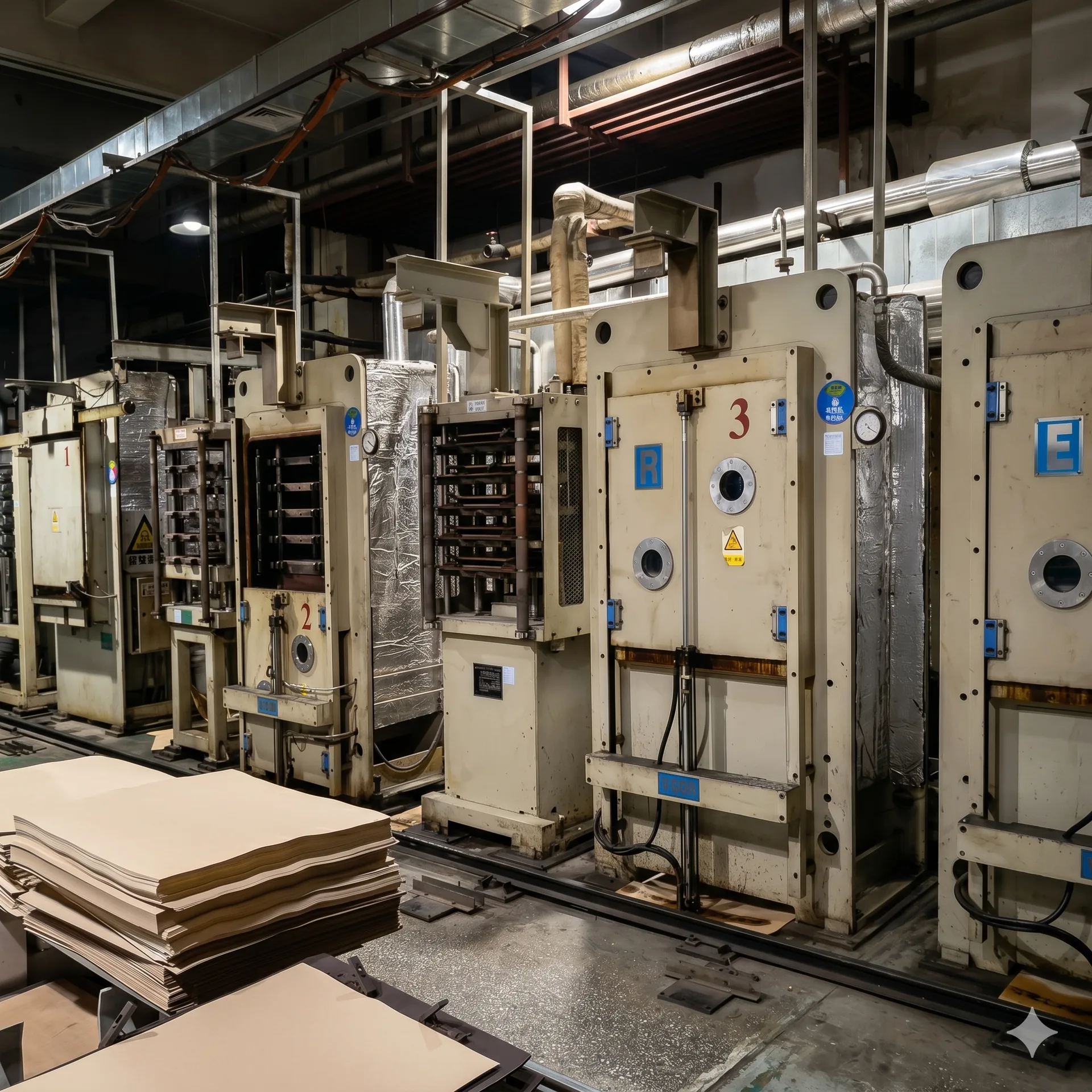
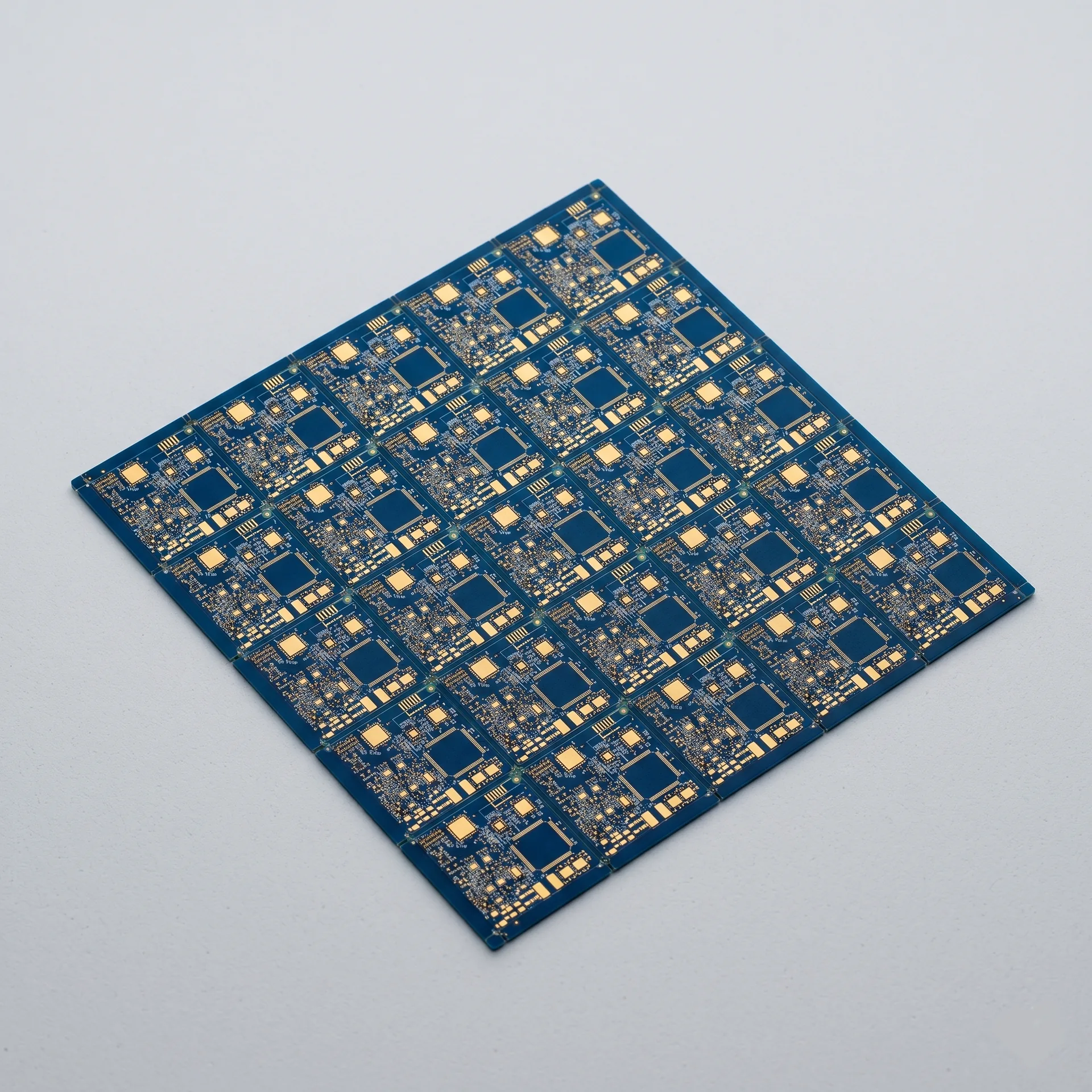
PCB fabrication with published limits up to 32 layers.
HDI, rigid-flex, heavy copper, and RF stackups with coupon impedance checks and DFM constraints you can use before file release.
- 32
- max layers
- 50 µm
- min trace / space
- ±5%
- impedance tolerance
- 12 : 1
- max aspect ratio
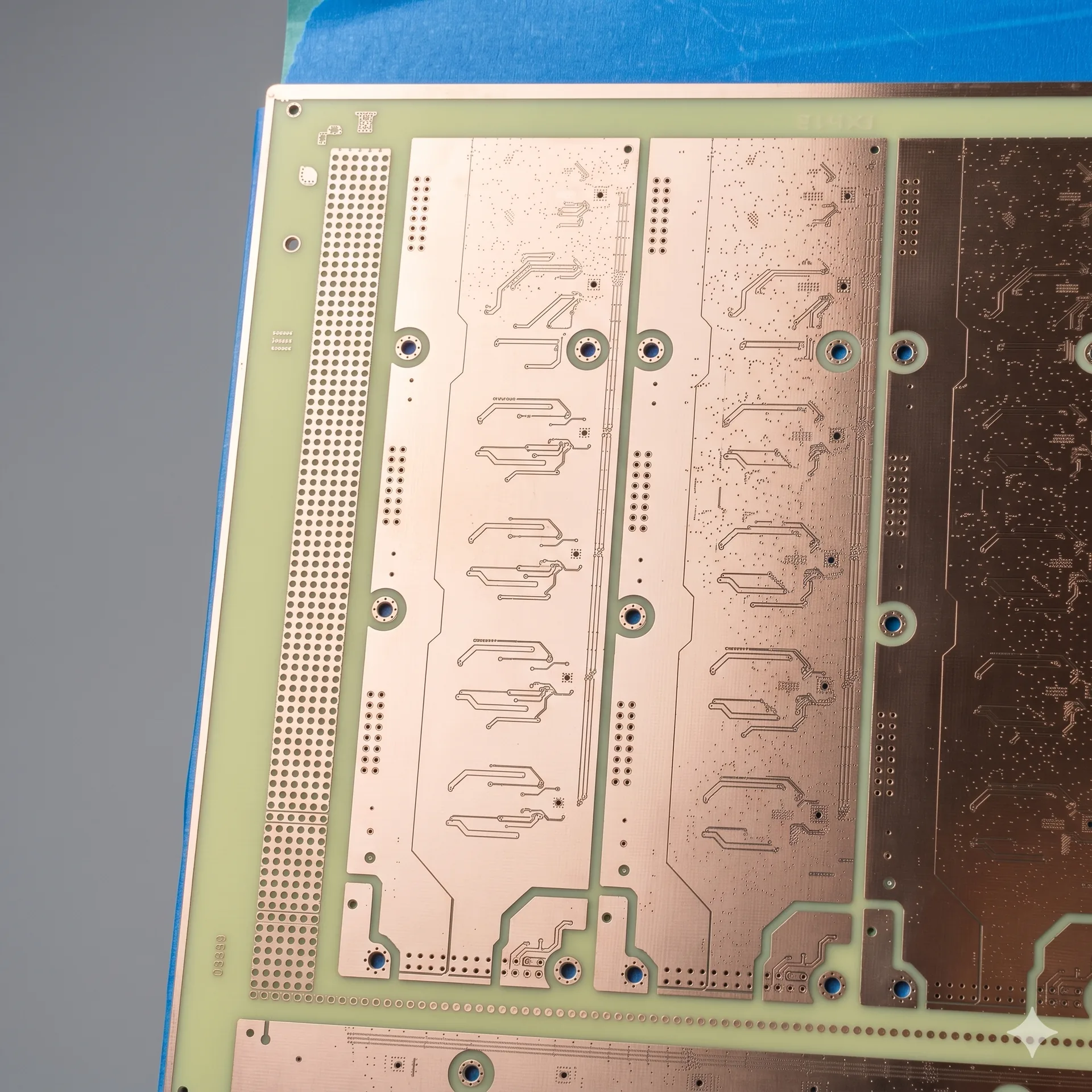
Stackup and technology
- Rigid, Flex and Rigid-Flex constructions.
- HDI with stacked or staggered microvias.
- Heavy Copper up to 6 oz inner / outer.
- High-frequency stackups (Rogers RO4350B / RO4003C, PTFE).
- Buried and blind vias supported.
- Edge plating and castellation supported.
Materials
| Standard FR4 / Halogen-free FR4 | Available |
|---|---|
| Mid-loss FR4 | For 10–25 G channels (e.g. IT-180A, IT-170GRA1) |
| Low-loss laminates | Megtron 6 / 7, EM-528K, Tachyon-100G |
| High-TG FR4 | Tg 170 °C / 180 °C |
| High-frequency | Rogers RO4350B, RO4003C, PTFE |
| Metal-core | Aluminum-base, Copper-base |
| Flex / Rigid-Flex | Polyimide |
Process limits
| Layer count | Up to 32 |
|---|---|
| Min trace / space | 50 / 50 µm |
| Min mechanical drill | 0.15 mm |
| Min laser microvia | 75 µm |
| Max aspect ratio | 12 : 1 |
| Board thickness | 0.2 mm to 6.4 mm |
| Max board size | 560 × 660 mm |
| Impedance tolerance | ±5% single-ended, ±7% differential |
| Min solder mask web | 75 µm |
| Min silkscreen line | 100 µm |
| Edge bevel angle | 20° / 30° / 45° / 60° |

Surface finishes — when to choose which
| ENIG | Default for fine-pitch BGA, repeated reflow, RoHS programs. |
|---|---|
| ENEPIG | Wire-bonding compatibility, gold bonding, longer shelf life. |
| OSP | Cost-sensitive consumer; sensitive to handling and storage time. |
| HASL Lead-Free | Standard for THT-heavy boards; not recommended for fine-pitch SMT. |
| Immersion Tin | Flat finish for press-fit and high-density SMT; storage-time-sensitive. |
| Immersion Silver | RF performance, tarnish-sensitive — needs sealed packaging. |
| Hard Gold | Edge connectors, switch contacts; do not use across full pad area (cost). |
Copper weights and current handling
| Standard outer copper | 1 oz / 35 µm |
|---|---|
| Heavy copper outer | Up to 6 oz / 210 µm |
| Inner layer copper | Up to 4 oz / 140 µm |
| Trace width for 1 A (1 oz, 30 °C rise) | ≈ 0.4 mm reference, board-specific |
| Combined heavy-copper outer + inner | Stackup review required |
Drilling, plating and via technology
- Mechanical drill from 0.15 mm; laser microvia from 75 µm.
- Stacked and staggered microvias supported (HDI builds).
- Filled and capped vias for via-in-pad designs (BGA).
- Controlled-depth (back-drill) drilling for stub removal on high-speed nets.
- Press-fit holes with controlled tolerances on request.
- Standard green LPI mask; black, white, blue, red, matte options on request.
- Min mask web 75 µm; min silkscreen line 100 µm.
- Mask-defined pads supported on customer request (review per program).
- Two-color silkscreen per panel supported on request.
- 100% electrical test (Flying Probe or Bed-of-Nails depending on volume).
- Impedance verification on separate TDR coupons.
- Microsection analysis on first-article samples.
- Cross-section on quality challenges, retained per program.
- IPC-A-600 Class 2 standard, IPC Class 3 on request.
What we need in the manufacturing package
- Gerber RS-274X with embedded apertures, or IPC-2581 / ODB++.
- Drill files (Excellon) with units and zero-suppression stated; or unified package.
- Stackup definition, including dielectric thicknesses if specified.
- Impedance targets per net class, with reference layer notes.
- Surface finish, copper weights and solder mask color.
- Panelization preference (single board, customer panel, fab panel).
- Special fab notes — back-drill targets, controlled-depth requirements, edge plating.
Design choices that affect cost and lead time
- Layer count is the strongest cost driver — collapsing by two layers via routing rework often beats material changes.
- Trace / space at the limit of process capability raises yield risk; staying one step back is cheaper across a series.
- HDI microvia counts (especially stacked) raise both cost and lead time; consider staggered alternatives.
- Heavy copper increases etching time and impedance tolerance widens; flag the trade-off early.
- Hard Gold across full areas is rarely justified — restrict to contact pads.
- Hybrid stackups (RF + digital) extend lead time; group RF area onto a daughter card if economically feasible.
Common pitfalls we see in incoming Gerber packages
- 1. Drill file with no units stated — interpretation defaults differ across CAM tools.
- 2. Impedance targets stated as a single number with no reference layer or net class.
- 3. Solder mask defined too tight on QFN ground pads — paste deposition cannot align reliably.
- 4. Silkscreen overlapping pads or gold fingers — operator complaints, customer rework on first article.
- 5. Stackup with no dielectric thickness — impedance cannot be verified before fabrication.
- 6. Edge plating not defined as a layer — assumed-vs-explicit divergence on first article.
Quality classes we run
| IPC-A-600 Class 2 | Standard for industrial / consumer / commercial. |
|---|---|
| IPC-A-600 Class 3 | On request — high-reliability programs (medical, aerospace context). |
| ESA / Mil contexts | Not run as a separate certification track. |
Next step
Send your manufacturing package to start scope review.