
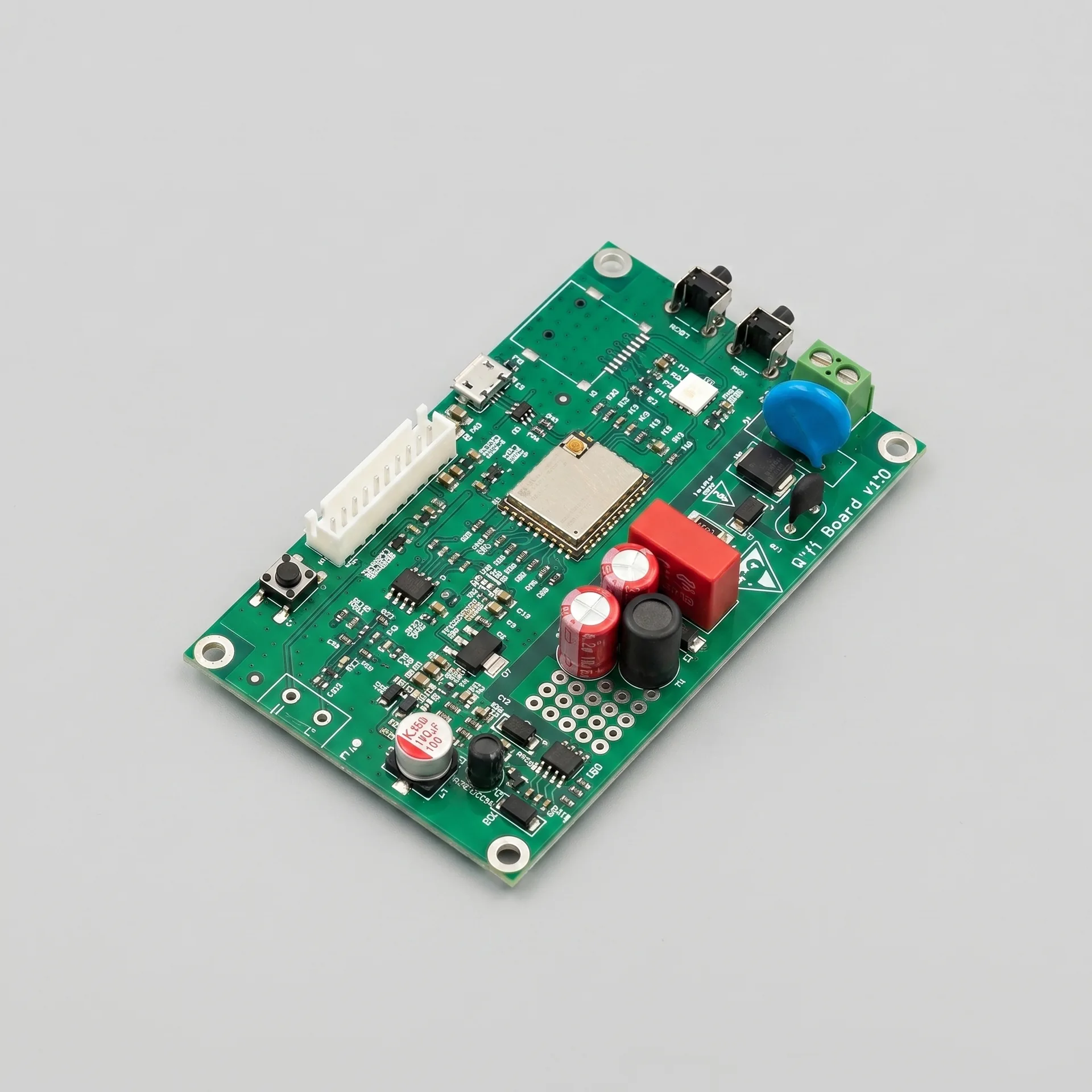
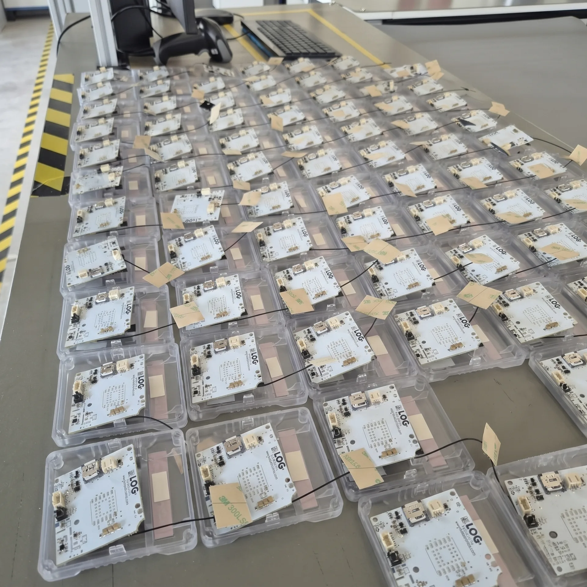
PCBA assembly from 01005 to fine-pitch BGA with test coverage.
SMT and THT assembly with SPI, AOI, X-Ray, ICT/FCT options, plus the manufacturing package rules that prevent avoidable ramp delays.
- 01005
- smallest component
- 0.3 mm
- min BGA pitch
- 100%
- SPI + AOI coverage
- ICT + FCT
- end-of-line test
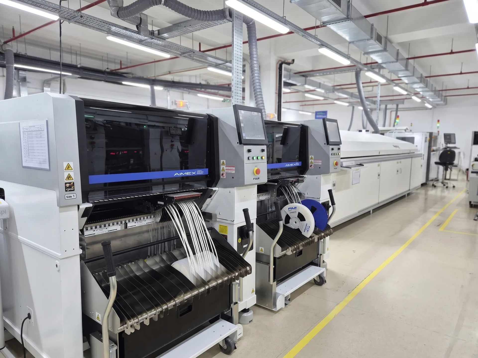
SMT assembly
| Min component | 01005 / 0201 |
|---|---|
| Min BGA / CSP pitch | 0.3 mm |
| Max board size | 460 × 510 mm |
| Min board size (with carrier) | 20 × 20 mm |
| Package-on-Package (PoP) | Supported |
| Double-sided assembly | Supported |
| Paste deposition | Stencil and jet-printed |
| Reflow zones | 10 to 12, nitrogen on request |
THT assembly
- Wave soldering with selective fingers.
- Selective soldering for mixed-tech boards with sensitive SMT neighbors.
- Manual assembly and rework for BGA, QFN, large connectors and mechanical hardware.
- Press-fit insertion with calibrated fixtures.
- Bonded heatsinks and stiffeners installed pre- or post-reflow as defined.
Coating, potting and underfill
- Conformal coating: acrylic, urethane, silicone, parylene.
- Selective spray, dip and brush application.
- Potting in customer-specified or in-house-made molds.
- Underfill for BGA and fine-pitch packages.
- First-article coating coverage photos as standard documentation.
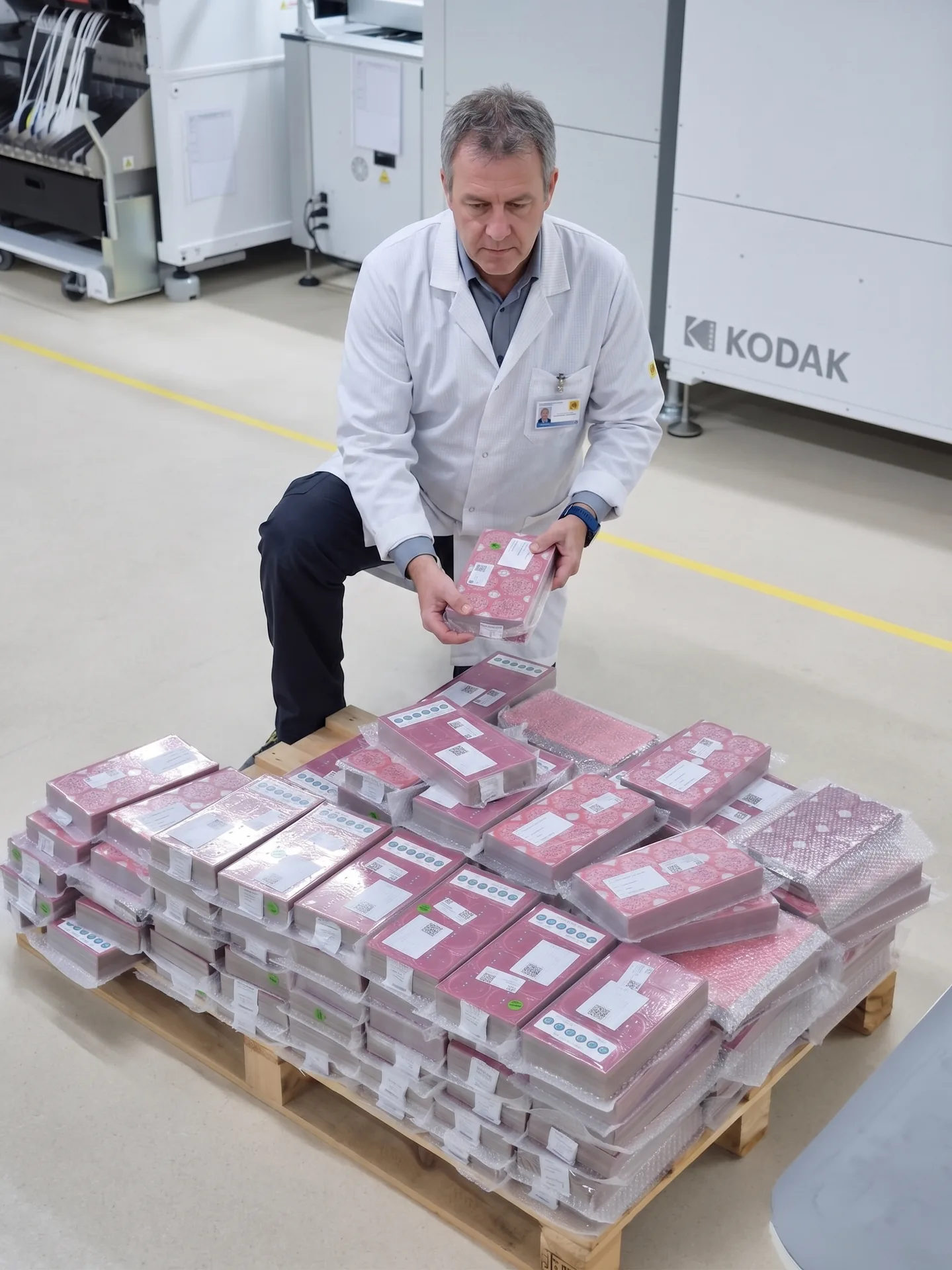

Flashing and serialization on the line
- MCU and Flash programming during the SMT or end-of-line stage.
- Laser marking of serial numbers, datamatrix and QR codes.
- IMEI / MAC / Bluetooth address provisioning from customer-managed pools.
- Certificate provisioning into secure elements.
- Per-unit log of programmed values against the serial.
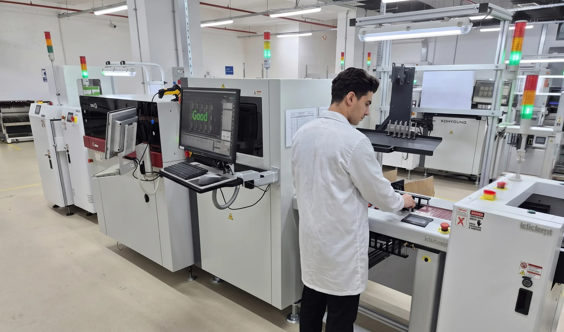
In-line inspection
- 3D SPI on every board after paste deposition.
- 3D AOI after reflow on both sides.
- X-Ray sampling for BGA and QFN voids; 100% on critical lots.
- Defect data sent to the MES at the unit level.
- First-Article Inspection (FAI) documented per revision.
Component handling — MSL, ESD, dry storage
- MSL-class components tracked through dry cabinets with floor-life logging.
- ESD wristbands and continuous monitoring on every workstation.
- Components stored in dry cabinets at < 5% RH for sensitive parts.
- Reel-to-shipment lot traceability per active part.
- Authenticity verification — active components sourced from authorized channels.
BGA assembly notes
- Reflow profile validated per BGA package — large body parts have non-trivial thermal lag.
- X-Ray sampling configurable from 10% to 100%; we recommend 100% on FCBGA.
- Voiding limits enforced per IPC-7095 (typical: < 25% per ball, no joining voids).
- Underfill on request — required where the board is exposed to mechanical shock.
- Rework supported with documented profile and post-rework X-Ray.
Fine-pitch and 01005 considerations
- 01005 placement requires controlled paste volume — 100% SPI is the only reliable check.
- Substrate flatness matters; warped substrate causes graping and tombstoning at high rates.
- Pad design should follow IPC-7351 nominal — non-standard pads cause repeatability issues.
- Avoid mixing 01005 and through-hole on the same side where possible.
What we need in the manufacturing package
- BOM in CSV or XLSX with reference designators, qualified MPN and qualified alternates.
- Pick-and-place file (CPL / XY data) with rotation convention and origin clearly noted.
- Assembly drawing with top / bottom views, polarity marks, fiducials, mechanical hold-down points.
- Conformal coating mask defined as a layer or as a clearly marked drawing — not as a free-text note.
- Test plan or FCT script outline; we co-design fixtures from this.
- Build instructions for hand-place / post-reflow components.
DFM checklist for PCBA
- At least three fiducials per board side, in non-symmetric positions.
- Test points exposed on a single side wherever possible.
- Component courtyards respected; minimum 0.5 mm between components for hand rework.
- Polarity marks on the silkscreen and inside the courtyard.
- Tooling / depanelization holes or v-score lines defined; sensitive components kept clear of stress paths.
- BGA placement allows enough clearance for X-Ray and rework.
Common pitfalls we see in BOMs
- 1. Single-source MPN with no alternate — first allocation event blocks the program.
- 2. Generic part description without an MPN — purchasing cannot resolve at quote time.
- 3. Mixed reel and tape-and-ammo packaging assumptions — line setup time grows.
- 4. BOM lines with `0R` resistors that should be DNP — production picks them up unless explicitly marked.
- 5. Quantity column missing for connectors — assembly drawing and BOM diverge on first article.
- 6. Polarity-sensitive parts (caps, diodes, LEDs) not marked in the BOM Notes column.
Test strategy choices
| AOI only | Lowest cost; catches most placement and joint defects; misses functional faults. |
|---|---|
| AOI + X-Ray sampling | Default for BGA-bearing boards; raises sample rate per program. |
| AOI + Flying Probe | Engineering builds, low / mid volume; no fixture investment. |
| AOI + ICT (Bed-of-Nails) | High-volume programs; fixture investment justified by repeated runs. |
| AOI + ICT + FCT | Default for safety-critical or high-margin programs. |
| FCT only | Possible when topology blocks ICT; coverage trade-off documented. |
Build types we run
| Turn-key | We source the BOM in full. |
|---|---|
| Consigned | Customer ships components; we run the line. |
| Partial consigned | Customer supplies long-lead or specialty components; we source the rest. |
| BOM-with-substitutions | We propose alternates against a customer-approved list. |
Lead-time drivers for PCBA
- Component lead time is usually the dominant factor — especially for active parts on allocation.
- Stencil fabrication and first-article setup add ~2–3 working days on a new program.
- FCT fixture design and validation add 1–3 weeks depending on test scope.
- Conformal coating and potting add a process day per batch.
- Programming on the line adds cycle time but rarely affects ship date.
Next step
Send your manufacturing package to start scope review.