
Telecom and networking PCB and PCBA with controlled impedance.
Switch, router, base-station, and optical platform boards with low-loss stackups, BGA-heavy assembly, and coupon-backed impedance reporting.
- 32
- max layers
- ±5%
- impedance tolerance
- 100%
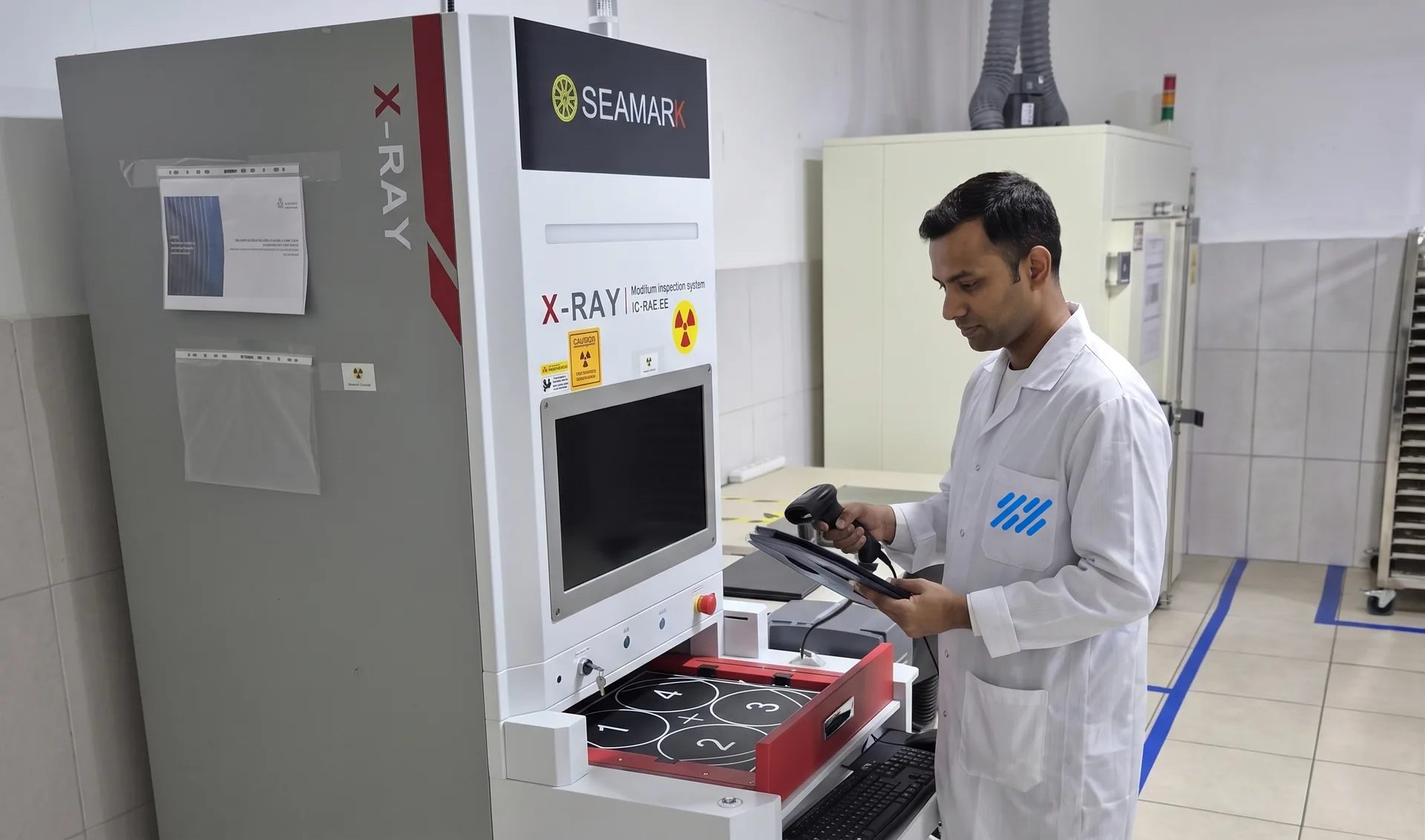
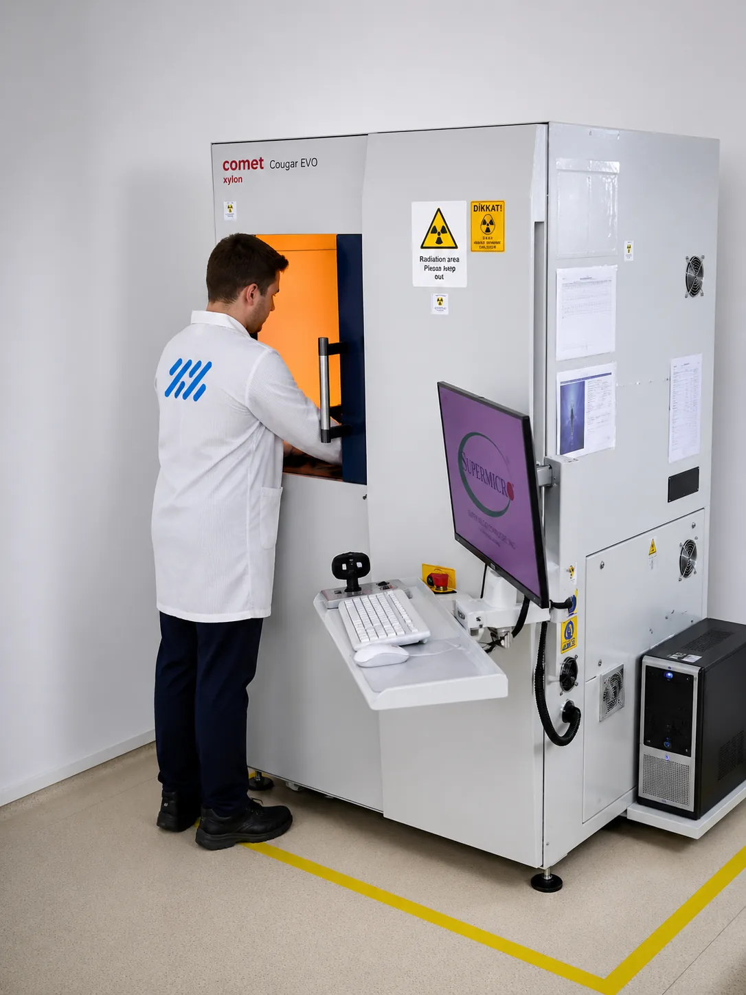
- X-Ray on BGA-dense lots
- FCBGA
- high-pin-count assembly
What we manufacture in this vertical
- PCB and PCBA for L2 / L3 switches and routers (top-of-rack to spine class).
- 5G base-station processor, RF and timing PCBA.
- Optical transceiver PCBA (SFP+, QSFP, QSFP-DD).
- Back-plane and midplane PCBA with high pin counts.
- SFP+ / QSFP cage soldering and front-panel daughter board PCBA.
Layer counts and material families typical in telecom
| Layer count | 8 to 32 |
|---|---|
| Standard FR4 | Mid-loss for 10 / 25 G channels |
| Low-loss laminates | Megtron 6 / 7, EM-528K, Tachyon-100G |
| High-frequency | Rogers RO4350B / RO4003C, PTFE for RF sections |
| Hybrid stackups | Supported (RF + digital on the same board) |


Signal integrity and impedance control
Impedance is a manufacturing outcome, not a wish. We treat it as a measured deliverable with a written tolerance window per net class.
TDR coupons designed into every panel and measured per net class.
Single-ended ±5%; differential ±7% standard. Tighter tolerances on request after stackup review.
Controlled-depth (back-drill) drilling for stub removal on high-speed nets.
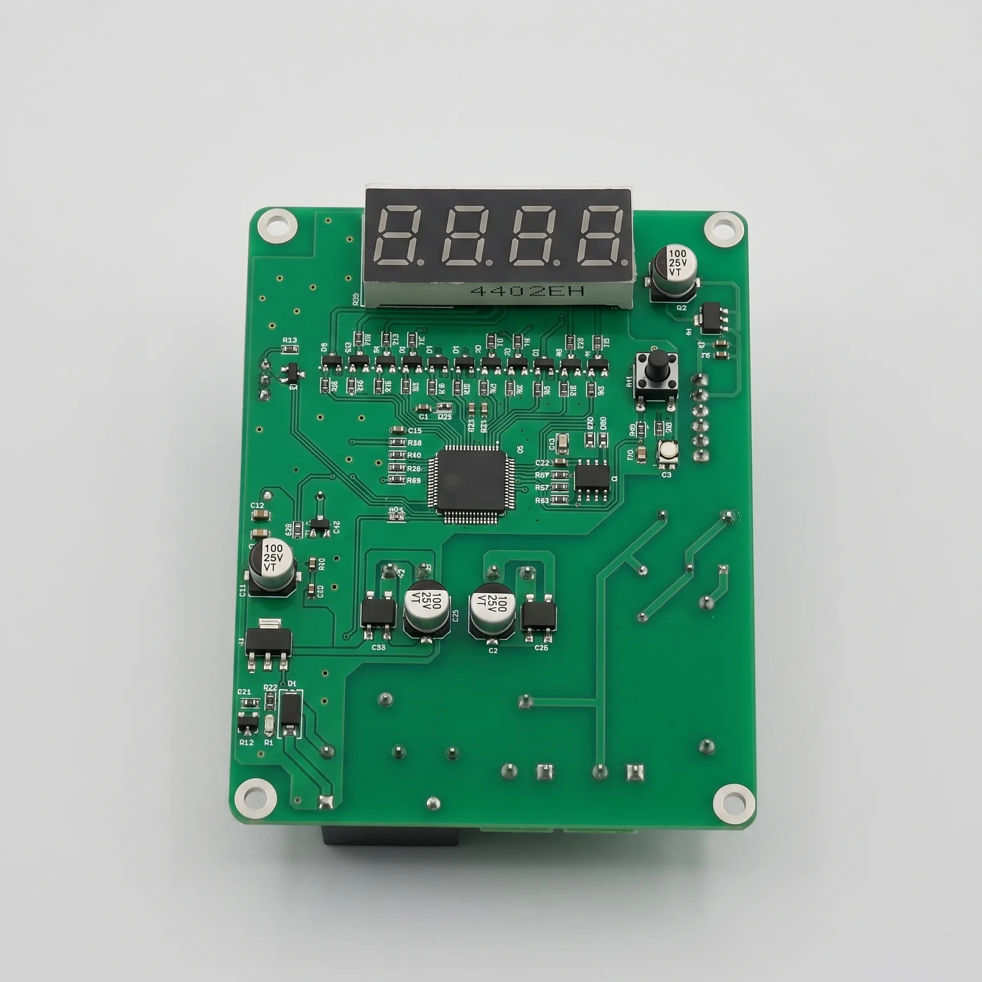
BGA and high-pin-count assembly
- FCBGA packages with 2,000+ pins assembled and X-Rayed at 100%.
- Voiding limits enforced per IPC-7095 (typical: < 25% per ball, no joining voids).
- Reflow profiles validated per package — surrogates used for new SKUs to protect the first real article.
- Underfill optionally applied for high-shock or high-thermal-stress programs.
- Rework on FCBGA supported with documented profile and post-rework X-Ray.
Thermal management at the board level
- Thermal pad placement and stencil aperture optimization for high-power devices.
- Heatsink retention assembly with calibrated torque drivers.
- Heat-spreader application with controlled bondline thickness.
- First-article thermal imaging on request to validate stack assembly.
What to think about before files arrive
- Provide impedance targets per net class as a written table — not as a single number on a notes page.
- Include a stackup proposal; expect us to propose modifications during review.
- Identify back-drill targets explicitly with depth tolerance.
- Mark BGA placement rules (minimum component-to-BGA edge clearance) for rework feasibility.
- Provide test coupon design or accept ours.
- Identify all controlled-impedance nets in the netlist export.
Documentation we produce per program
- Stackup confirmation with measured Dk / Df notes.
- Impedance test report per panel from TDR coupons.
- X-Ray report on every BGA-dense lot.
- Microsection report on first article (where requested).
- FCT logs per serial.
Common pitfalls we see in telecom handoffs
- 1. Impedance targets stated for the design layer but no coupon defined — we cannot certify what is not measurable.
- 2. Routing on the surface layer for sensitive high-speed nets — insertion loss exceeds budget at the first article.
- 3. BGA placement too close to a stiffener or board edge — rework not feasible without damaging adjacent parts.
- 4. No back-drill specified on long via stubs — eye height fails on the first SerDes link test.
- 5. Underfill assumed but not specified — ramp planning assumes a process step we do not run.
Representative cases
- 24-layer L3 datacenter switch PCBA — FCBGA switch silicon, SFP+ cage soldering, full-load stress testing.
- 5G base-station processor board on a controlled-impedance backplane.
- QSFP-DD optical transceiver PCBA on Megtron 6, with hybrid RF + digital stackup.
Next step
Send your manufacturing package to start scope review.